
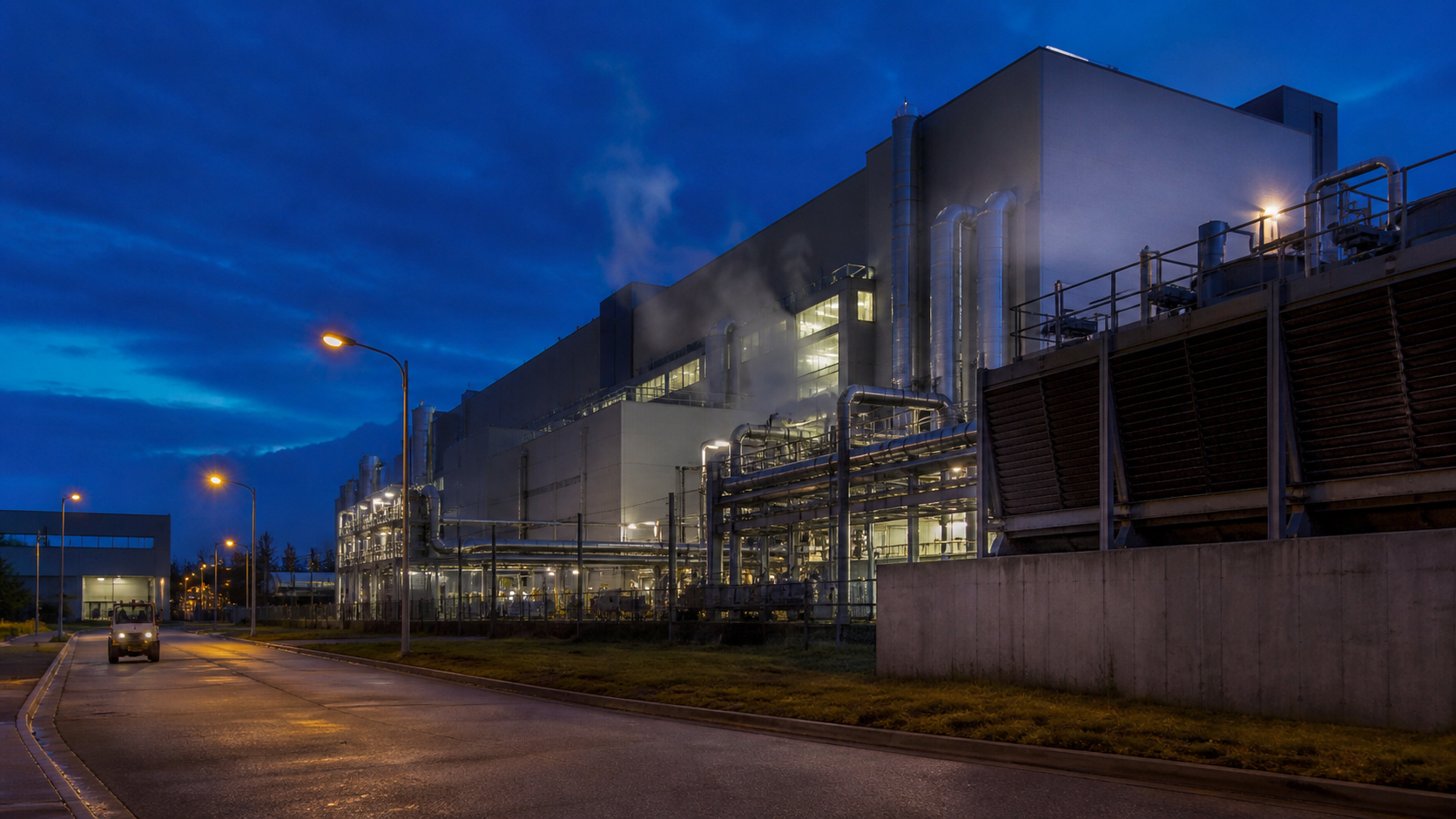
Taiwan Semiconductor Manufacturing Company (TSMC) is expanding outside Taiwan, but “more global” does not mean that every factory can make the same chips. Its 2025 annual report and July 2026 earnings materials describe a network with different process nodes, end markets and construction stages.
This guide compares TSMC’s manufacturing footprint in Taiwan, Arizona, Japan and Europe. The practical answer is that Taiwan remains the center of advanced scale, Arizona adds leading-edge capacity for US customers, Japan is building a mixed specialty-and-advanced site in Kumamoto, and Dresden is aimed at automotive and industrial demand. The footprint is diversifying, but it is not yet a simple substitute for Taiwan.
Key Takeaways
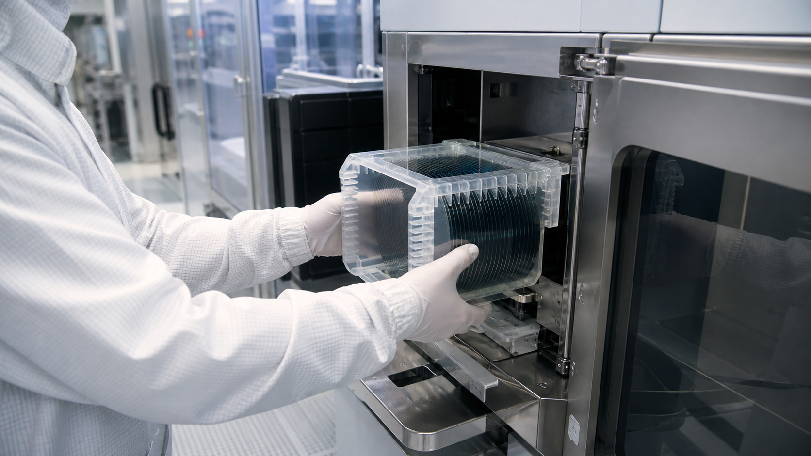
- TSMC reported more than 17 million 12-inch-equivalent wafers of annual capacity in 2025, with Taiwan still hosting the largest and deepest manufacturing base.
- Arizona’s first fab entered high-volume 4nm production in the fourth quarter of 2024. Its second fab is being fitted for 3nm and more advanced technologies, while a third began construction in 2025.
- Japan’s JASM site in Kumamoto began volume production in late 2024. Its second fab is under construction and is planned to add 3nm capability alongside specialty nodes.
- Dresden is a specialty-technology project for automotive and industrial applications, not a copy of Taiwan’s leading-edge GIGAFAB network.
- For investors and technology buyers, the useful question is not simply “How many fabs does TSMC have?” It is which node, product family, customer demand and completion milestone each location supports.
How TSMC’s Global Fab Network Is Structured
TSMC’s business is a contract foundry model: customers design chips, while TSMC manufactures them using a wide range of process technologies. A fab’s location therefore matters alongside its node, packaging links, utilities, workforce and customer qualification.
In 2025, TSMC said its managed facilities exceeded 17 million 12-inch-equivalent wafers of annual capacity. It manufactured 12,682 products using 305 distinct process technologies for 534 customers. The company also said advanced technologies of 7nm and beyond accounted for 74% of wafer revenue.
Those figures show why a site count can mislead. A 12-inch fab running mature automotive processes is not interchangeable with a high-volume 3nm facility. Nor does land purchased for a future phase equal installed capacity today.
Swipe horizontally to view all columns.
| Region | Disclosed role | Status and process signal | What it does not prove |
|---|---|---|---|
| Taiwan | Core GIGAFAB network and advanced-node expansion | Multiple 2nm phases planned in Hsinchu and Kaohsiung; advanced packaging also expanding | That every Taiwan site is dedicated to 2nm |
| Arizona, United States | Leading-edge capacity closer to US customers | Fab 1 in 4nm high-volume production since Q4 2024; Fab 2 being fitted for 3nm and more advanced technologies; Fab 3 under construction in 2025 | That the full planned cluster is already operating |
| Kumamoto, Japan | Specialty technology and additional advanced capacity | JASM Fab 1 in volume production since late 2024; Fab 2 under construction, with 3nm planned alongside specialty nodes | That Japan replaces Taiwan for the whole product portfolio |
| Dresden, Germany | Specialty technology for automotive and industrial use | Construction began in 2024; technology focus is specialty, automotive and industrial | That Europe will immediately supply leading-edge AI accelerators |
The table is a snapshot from company disclosures, not a production forecast. TSMC’s project descriptions can change as customer demand, government support, construction and qualification develop.
Taiwan Remains the Advanced-Scale Anchor
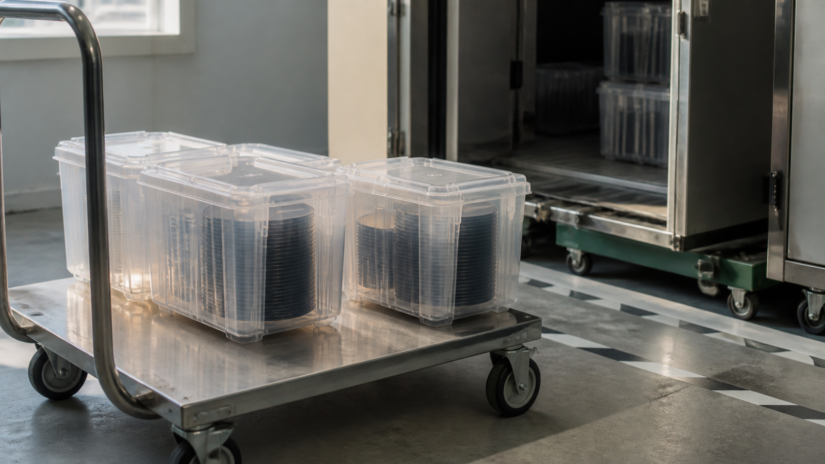
TSMC’s annual report describes four 12-inch GIGAFAB facilities, four 8-inch fabs and one 6-inch fab in Taiwan. The company is preparing multiple phases of 2nm fabs in Hsinchu and Kaohsiung and continuing to invest in leading-edge and advanced-packaging facilities across several locations.
This concentration brings operating advantages. A dense manufacturing base can share engineering knowledge, suppliers and yield-learning systems. It also allows TSMC to balance demand across facilities more flexibly than a single isolated overseas fab.
The risk is concentration. A global customer may want geographic flexibility, but qualification is specific to a product and process. Moving a design between nodes or fabs can require engineering work, new masks, testing and customer approval. Geographic diversification can therefore reduce some disruption exposure without eliminating Taiwan dependence.
For readers tracking the network, the relevant Taiwan milestones are 2nm ramp timing, advanced-packaging expansion, capacity utilization and the mix of high-performance-computing demand. None should be treated as a standalone signal for TSMC’s share price.
Arizona Adds Leading-Edge Capacity, Gradually
TSMC Arizona’s first facility began high-volume production of 4nm technology in the fourth quarter of 2024, according to the annual report. The second facility had completed construction and was in the process of installing systems for 3nm and more advanced technologies. TSMC also began construction of a third facility in 2025 and described plans for additional fabrication plants, advanced packaging and a major research-and-development center.
The distinction between operating, fitting-out and planned capacity is important. A construction announcement expands the possible future footprint; it does not equal qualified wafer output. A customer also needs confidence in yield, delivery, cost and ecosystem support before treating a new site as interchangeable with an established Taiwan line.
TSMC’s Q2 2026 earnings transcript provides a second lens. Management raised the 2026 capital budget to US$60 billion–US$64 billion because of what it called strong structural customer demand, including emerging agentic-AI demand. The planned allocation was 70–80% to advanced process technologies, about 10% to specialty technologies and 10–20% to advanced packaging, testing, mask making and other work.
That allocation supports the interpretation that Arizona is part of a broader advanced-capacity build-out. It does not identify how much of the company’s total output will move to the United States or guarantee a completion date for every announced phase.
Japan’s Kumamoto Site Has a Different Mix
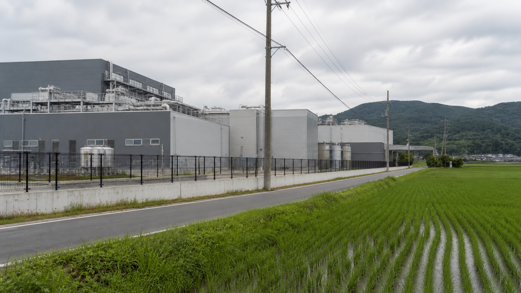
Japan Advanced Semiconductor Manufacturing (JASM) is TSMC’s majority-owned manufacturing subsidiary in Kumamoto. Its first fab entered volume production at the end of 2024. The second fab began construction in 2025 and is planned to use 3nm technology as well as specialty nodes.
The planned two-fab Kumamoto site is designed to serve automotive, industrial, consumer-electronics and high-performance-computing applications. That mix matters for international readers: Japan’s role is not merely a symbolic “friend-shoring” location. It is a manufacturing site tied to customers and supply chains in a major industrial economy.
At the same time, JASM should not be described as a miniature version of Taiwan’s entire network. TSMC’s own disclosures show a narrower site role and a different combination of nodes. The correct comparison is capability by product and process, not country against country.
Japan also adds a useful regional perspective. A Kumamoto site can shorten some supply-chain links for Japanese automotive and industrial customers, while still relying on TSMC’s wider global engineering, equipment and materials ecosystem. Its value is therefore partly local resilience and partly integration with the larger network.
Europe Is Focused on Specialty Manufacturing
TSMC began construction of a specialty-technology fab in Dresden, Germany, in 2024. The annual report identifies automotive and industrial applications as the focus.
This is a different demand problem from the leading-edge AI race. Automotive and industrial customers often value long product lifecycles, qualification stability, reliability and secure supply as much as the smallest available node. Dresden can therefore expand TSMC’s regional relevance without needing to compete directly with Taiwan’s most advanced logic production.
The project also shows why “global fab count” is a weak summary metric. A specialty fab can be strategically important even when it is not producing 2nm processors. Readers should monitor construction progress, technology qualification and customer commitments rather than assume that every overseas project has the same economic profile.
What the Footprint Changes—and What It Does Not
The build-out changes three practical things.
First, customers gain more options for manufacturing location. That can matter for supply-chain design, government incentives, logistics and business continuity. Second, TSMC can place selected capacity closer to major customer clusters. Third, the company creates a larger platform for matching process technology to end-market requirements.
But the build-out does not mean that supply-chain risk disappears. Advanced chips require specialized equipment, materials, software, packaging and engineering skills. A wafer made outside Taiwan can still depend on the same global ecosystem. New fabs also face construction, labor, utilities, yield-learning, cost and qualification risks.
The most defensible conclusion is narrower: TSMC is building geographic redundancy around a Taiwan-centered manufacturing system. That may improve resilience over time, but the degree of independence must be measured by process, product and qualified volume.
A Practical TSMC Footprint Checklist
When TSMC publishes a new project update, use this sequence:
1. Identify the stage: announced, land acquired, construction started, construction completed, equipment installation, qualification or volume production. 2. Record the process node and product purpose. “Advanced” and “specialty” are not interchangeable labels. 3. Check whether the figure is capacity, annualized capacity, wafer starts or revenue mix, and keep the period attached. 4. Separate management plans from results already reported in the annual report or quarterly release. 5. Ask which ecosystem elements remain shared across regions: equipment, packaging, materials, engineering and customer qualification. 6. Recheck the next quarterly presentation for schedule changes, capital spending and customer-demand language.
For a market reference, the NYSE-listed American depositary receipt (ADR) is shown below. One ADR represents an interest in the Taiwan-listed ordinary shares through a depositary arrangement; it is not the same trading instrument as Taiwan-listed share 2330.
The chart is a market-data reference, not evidence that a fab milestone predicts a particular price. TSMC’s operating disclosures and risk factors should remain the starting point for research.
The Bottom Line for International Readers
TSMC’s Arizona, Japan and Europe projects are meaningful because they add different kinds of capacity to a global foundry network. Taiwan remains the scale and advanced-technology anchor. Arizona is moving from a first 4nm fab toward additional leading-edge capacity. Kumamoto combines specialty manufacturing with a planned 3nm expansion. Dresden is designed around automotive and industrial demand.
The best way to follow the story is to replace the headline question “How many fabs does TSMC have?” with four narrower questions: Which region? Which node? Which customer use case? Which construction or qualification stage? That framework will remain useful after the next capex headline fades.
Sources
- TSMC 2025 Annual Report — facility inventory, capacity, process and overseas-project disclosures.
- TSMC 2026 Q2 Quarterly Results — Q2 results, guidance and official presentation materials.
- TSMC Q2 2026 Earnings Call Transcript — 2026 capital-budget range and allocation.
- TSMC 2025 20-F — facility and risk disclosures.
This article is for informational purposes only and does not constitute investment advice.

