
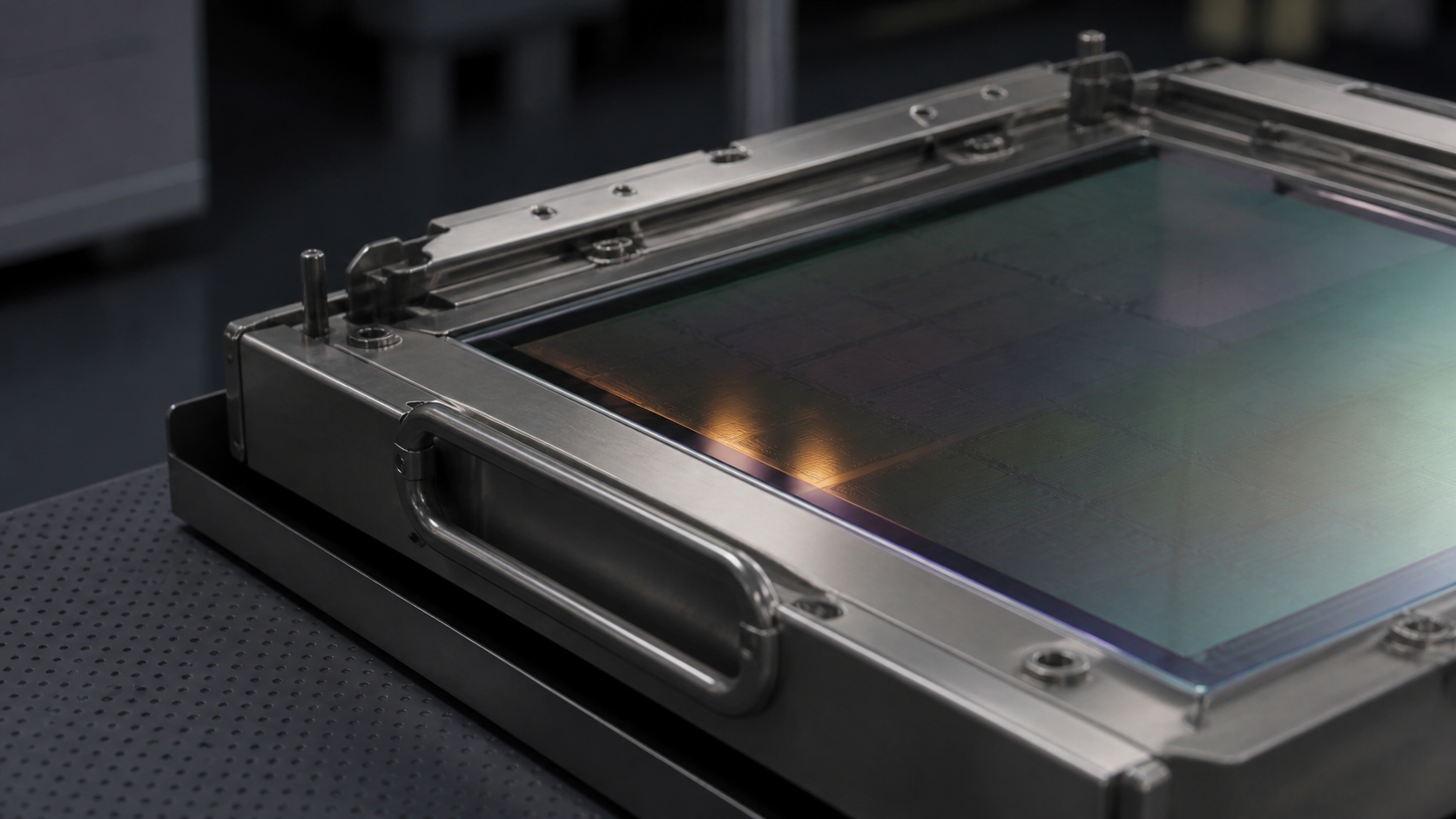
ASML’s High-NA EUV platform matters because it offers chipmakers a different way to print their most difficult layers: higher-resolution imaging can replace some multi-patterning steps. It does not mean that every advanced chip is already made with the new tool, or that a machine delivery proves broad commercial production.
The practical way to read the transition is to separate the technology claim from the adoption evidence. ASML’s EXE platform raises numerical aperture (NA) from 0.33 in its NXE EUV tools to 0.55. NA is an optical measure that affects how finely a lithography system can image a pattern. ASML says its EXE systems use 13.5-nanometer extreme ultraviolet (EUV) light and are designed for 8 nm resolution, versus 13 nm for the NXE platform. ASML’s EUV platform overview is the primary reference for those product definitions.
Key takeaways
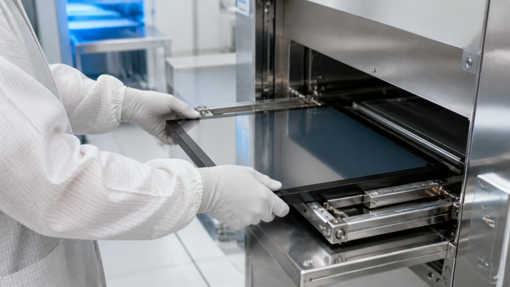
- High-NA EUV is a 0.55-NA optical platform, not a synonym for every sub-2 nm chip.
- Its main economic promise is fewer patterning steps on selected layers, not a guaranteed density result across an entire processor or memory chip.
- ASML’s 2025 report records four 0.55-NA systems shipped to customer R&D facilities; that is meaningful deployment evidence, but it should not be relabeled as industry-wide high-volume manufacturing.
- The next evidence to watch is a named customer, node and layer with a disclosed production qualification—not a general AI-demand headline.
High-NA EUV is a new process option, not a node name
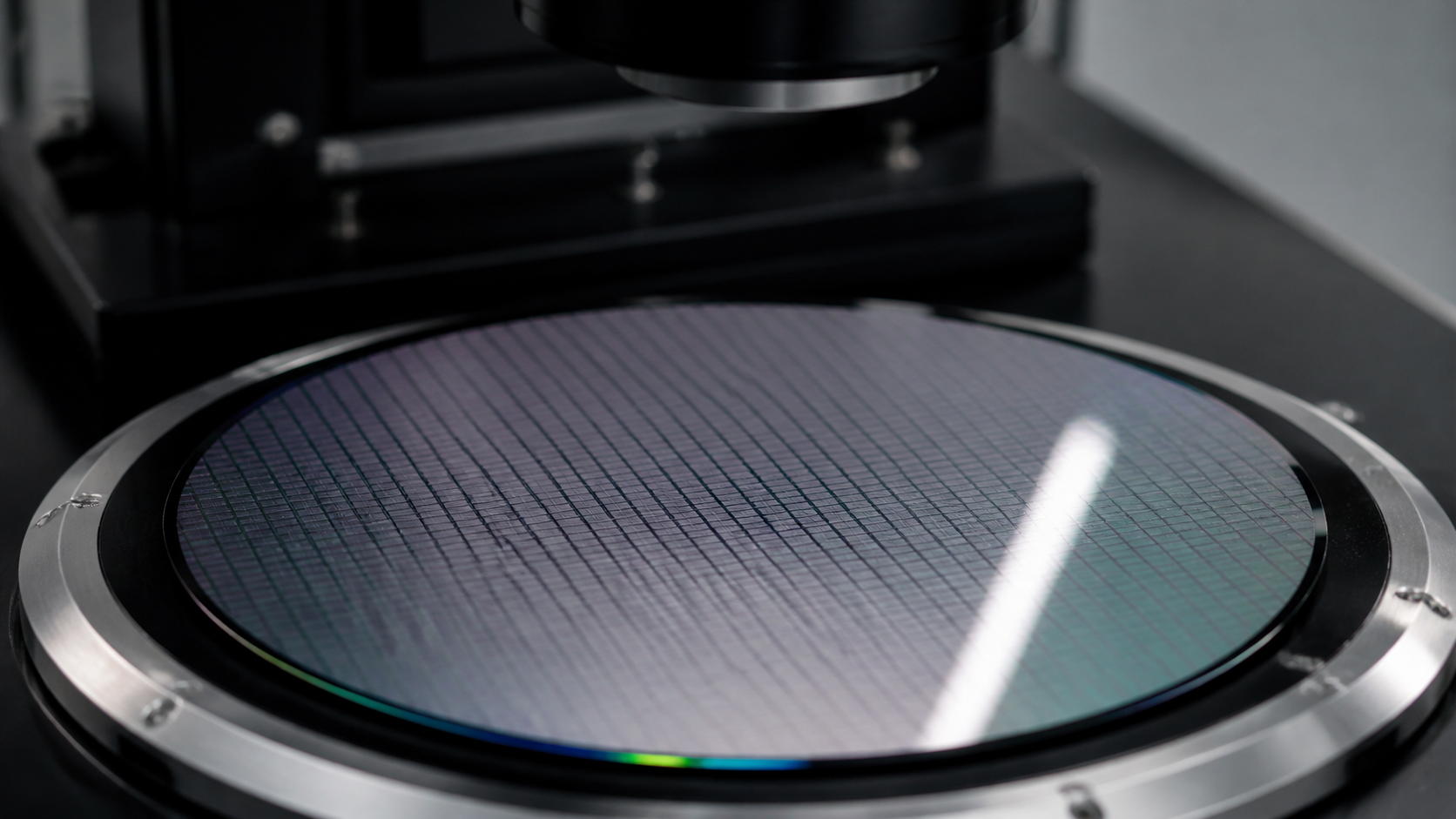
EUV lithography uses a very short wavelength of light to transfer patterns onto a wafer. At the leading edge, a chipmaker may need multiple exposures and processing steps to achieve a required pattern. ASML says the EXE:5000’s 0.55-NA optics can print features in a single exposure that are 1.7 times smaller than those possible with its NXE systems. It also says the comparison can support 2.9 times higher transistor density and 40% more imaging contrast. Those are ASML’s product claims under its stated reference conditions; they are not a blanket result for every design. The EXE:5000 product page sets out the company’s specifications.
The reader payoff is a cleaner question: which layer benefits enough to avoid extra patterning, and at what factory throughput and yield? A “2 nm” or “angstrom” label alone cannot answer it. Foundries can use different design rules, libraries and process flows, while logic and memory have different patterning needs.
Swipe horizontally to view all columns.
| ASML platform | Numerical aperture | Stated resolution | What changes | Important limit |
|---|---|---|---|---|
| NXE EUV | 0.33 | 13 nm | Established EUV platform for advanced logic and memory layers | It may still require multi-patterning for selected future features |
| EXE High-NA EUV | 0.55 | 8 nm | Higher contrast and smaller single-exposure features; ASML says this can simplify selected process flows | A high-NA tool does not itself disclose yield, volume or a chip’s full process flow |
ASML explains that the higher NA comes with new anamorphic optics. Those optics preserve traditionally sized reticles—the masks used to carry a layer’s pattern—but reduce the exposure field to half the NXE field. The system therefore uses faster wafer and reticle stages to keep productivity economically viable. That is why the transition is an engineering-and-factory question, not simply a sharper-image story.
Why 0.55 NA can reduce steps—and add constraints

The attraction of High-NA EUV is the possibility of single patterning where an older flow might need multiple patterning. Fewer steps can reduce cycle time and the number of opportunities for alignment or defect problems. ASML’s 2025 annual-report materials describe the potential for process simplification and lower resource use per wafer compared with multi-patterning on 0.33-NA EUV. That is a process-level comparison, not a promise that a new scanner uses less energy than an older one in isolation.
The constraints are just as important. The half-size field can make layout choices, reticle strategy and stage productivity relevant to economics. The tool must also be integrated with resist chemistry, metrology, inspection and yield learning. A factory cannot convert a vendor’s resolution figure directly into sellable chips.
This distinction helps when comparing ATG Press’s TSMC fab-footprint guide with a lithography article. A fab location tells readers where capacity is being built; a High-NA guide explains one of the process choices that could be qualified inside a fab. They answer different questions.
The adoption evidence ladder
For a fast-moving technology, the safest reading method is to label the evidence correctly.
Swipe horizontally to view all columns.
| Evidence level | What it establishes | What it does not establish |
|---|---|---|
| Product specification | The supplier’s designed capability and stated comparison | A customer’s actual yield or cost |
| Tool delivery or installation | A customer or research site can begin integration work | Commercial output at scale |
| R&D-fab deployment | Process and ecosystem learning can occur on the tool | A named product’s revenue contribution |
| Revenue recognition | The supplier has met its accounting criteria for a system sale | The recipient’s production ramp or demand durability |
| Named production qualification | A disclosed layer, node and product have passed a defined production milestone | The economics of every product or customer |
ASML’s 2025 Annual Report says it recognized revenue for four 0.55-NA systems shipped to customers’ R&D facilities, and that the first full-specification EXE:5200B was delivered to a customer. That is concrete progress through the delivery and R&D stages. It does not identify a universal production milestone for all recipients.
Intel’s High-NA EUV press kit provides another useful label: in April 2024, Intel said its system installation was complete and calibration had begun at D1X in Hillsboro, Oregon. In March 2026, imec said it had received an EXE:5200 for research access alongside patterning and metrology tools. These are meaningful development milestones, but neither should be turned into an unverified claim about every chipmaker’s high-volume production.
What ASML’s latest results do—and do not—say
ASML reported €9.326 billion of Q2 2026 net sales and €2.918 billion of net income in its July 15 release. The company linked its stronger outlook to AI-related investment and advanced logic and memory demand. It also said it planned to add roughly 30% to its 2026 low-NA EUV capacity for 2027. ASML’s Q2 2026 results are useful current context for the broader lithography cycle.
But low-NA capacity is not a High-NA shipment forecast. Readers should resist filling that gap with an assumed EXE-unit total, a customer ranking or a timetable. The relevant High-NA signals are narrower: new EXE deliveries, disclosed customer qualifications, measurable tool productivity and evidence that a layer’s simplified flow works at the needed yield.
For market context only, the U.S. instrument in the chart below is ASML Holding N.V.'s Nasdaq-listed sponsored ADR (`NASDAQ:ASML`), not a source for technology, delivery or adoption claims. Chart data may be delayed.
For a broader demand lens, see ATG Press’s NVIDIA revenue breakdown. AI-server demand can influence leading-edge logic and memory investment, but it does not remove the fab-level qualification work between a semiconductor-equipment order and commercial output.
A practical checklist for following High-NA EUV
When a company or supplier makes a High-NA announcement, check five things:
- Tool and platform: Is the disclosure about an EXE:5000, EXE:5200B or a different EUV platform?
- Stage: Does it say delivery, installation, calibration, R&D use, qualification or high-volume production?
- Layer and node: Is a specific layer or process node named, or is the language broad?
- Factory evidence: Are throughput, yield, defectivity, overlay or cycle-time results disclosed with definitions?
- Economic boundary: Is a vendor comparison being presented as a specification, or as a demonstrated customer result?
That checklist will stay useful as system generations and customer roadmaps move. It also keeps a clear line between a supplier’s technical claim, a company’s operational progress and an investor’s interpretation.
What to watch next
The most informative next disclosures would be a customer naming a High-NA-qualified layer and product, ASML reporting additional EXE-system revenue with an adoption-stage description, or a research partner publishing process results with explicit production limits. Conversely, a broad AI-capex headline, an EUV market-total figure or a single tool installation should be treated as context—not as proof that High-NA EUV has become standard across leading-edge manufacturing.
Sources
- ASML: EUV lithography systems — accessed September 1, 2026.
- ASML: TWINSCAN EXE:5000 — accessed September 1, 2026.
- ASML: 2025 Annual Report — published February 25, 2026.
- ASML: Q2 2026 financial results — published July 15, 2026.
- Intel: High-NA EUV press kit — published April 18, 2024.
- imec: EXE:5200 High-NA EUV system — published March 18, 2026.
This article is for informational purposes only and does not constitute investment advice.

