
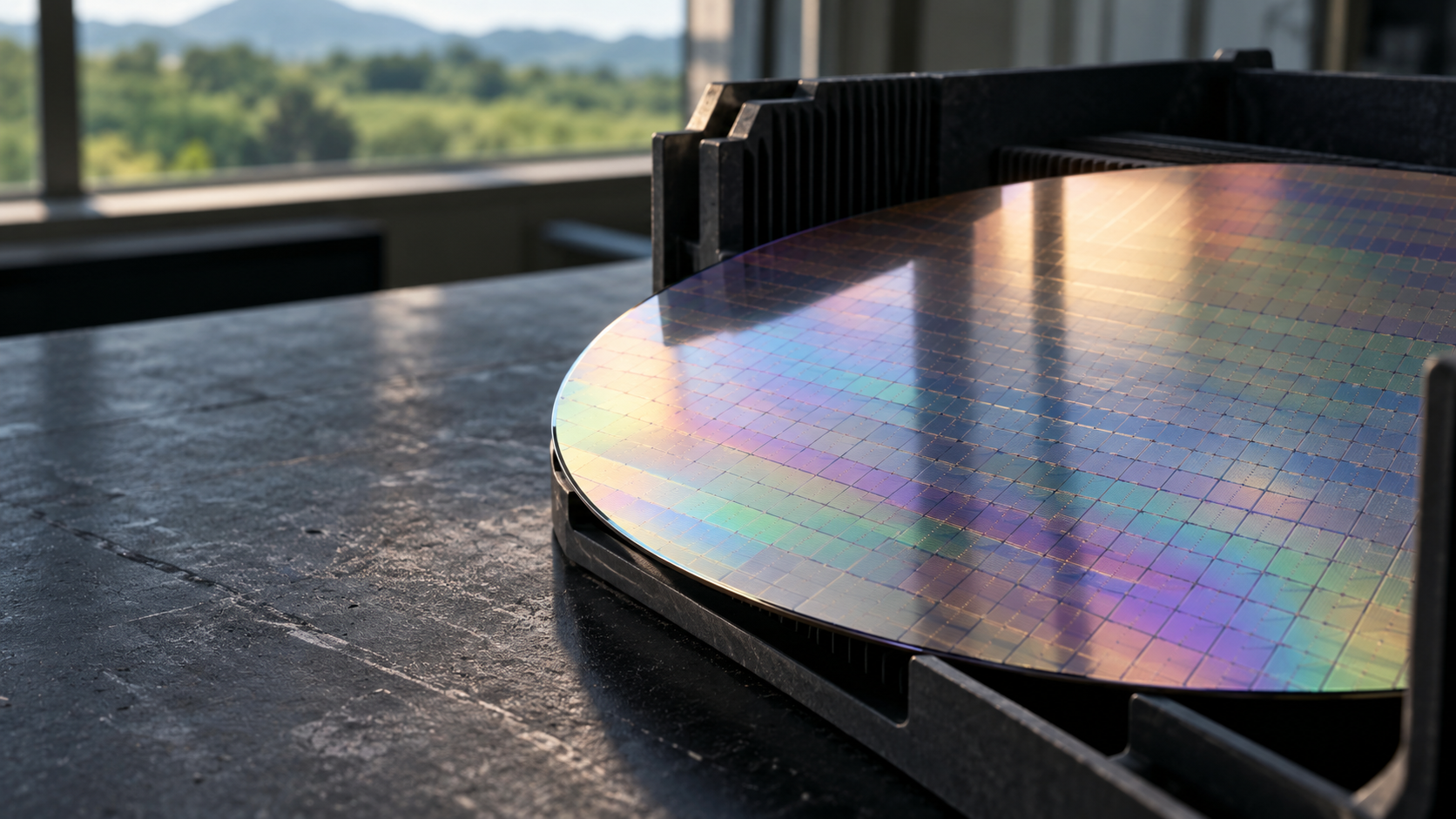
TSMC has confirmed that its second Kumamoto fab in Japan is planned to use 3-nanometer process technology and begin volume production in 2028. The useful reading is not simply “Japan gets 3nm”: the revised plan points to a smaller, higher-value capacity step than the earlier Fab 2 outline. It strengthens Japan's place in TSMC's global manufacturing map, but it does not by itself reveal customers, utilization, profitability or an investable outcome.
Key Takeaways
- TSMC said on 2026-10-15 that the second Japan fab is progressing toward 3nm use, with volume production scheduled for 2028.
- A recent Japanese technology-trade report on the approved plan says Fab 2 is set for 6,000 300mm-wafer-equivalent wafers a month and first shipments in Q4 2028; treat those as plan parameters, not a production forecast.
- The earlier Fab 2 design was a broader-volume plan. The new direction changes the technology mix and the scale, so old capacity figures should not be carried into current analysis.
- International readers should track construction, the first-shipment timetable, disclosed customer or product information and TSMC's next official updates—not infer all of those from the node name alone.
What changed at Kumamoto Fab 2
The confirmed change is straightforward: TSMC now plans to use its 3nm process technology at the second fab of Japan Advanced Semiconductor Manufacturing (JASM), its majority-owned manufacturing subsidiary in Kumamoto Prefecture, with volume production scheduled for 2028. TSMC made that statement in its 2026 Q3 earnings-call materials on 2026-10-15.
That replaces the practical context investors had been using. TSMC's February 2024 expansion announcement described Fab 2 as a 2027 project covering 6/7nm, 12/16nm and, in the combined Kumamoto-site plan, other mature nodes. The company has since moved to a 3nm plan; the 2024 release is therefore historical context, not current guidance.
Swipe horizontally to view all columns.
| Item | Earlier Fab 2 context | Current confirmed or reported plan | Why it matters | Source |
|---|---|---|---|---|
| Main technology | 6/7nm and 12/16nm in TSMC's 2024 outline | 3nm, confirmed by TSMC | A leading-edge node changes the type of capacity being discussed. | TSMC 2024 release; TSMC Q3 2026 transcript |
| Volume-production timing | By end-2027 in the 2024 outline | 2028, confirmed by TSMC | The start date moved; a reader should use the later company statement. | TSMC 2024 release; TSMC Q3 2026 transcript |
| Approved-plan capacity | 48,000 300mm-wafer-equivalent wafers/month reported for the previous Fab 2 plan | 6,000 wafers/month reported for the revised plan | Node leadership and wafer volume are separate questions. | EE Times Japan report on the METI plan |
| First shipment | Not the current reference point | Q4 2028 reported in the approved-plan overview | A more precise milestone to monitor than a generic 2028 label. | EE Times Japan report on the METI plan |
The 6,000-wafers-per-month figure and Q4 2028 first-shipment expectation come from an EE Times Japan report on the Ministry of Economy, Trade and Industry plan overview, published 2026-10-19. They are useful public-plan parameters, but not a TSMC sales forecast. TSMC's own October material confirms the node and 2028 volume-production timetable without publishing those parameters in the cited transcript.
Why “3nm” is not the whole answer
`3nm` is a process-node label: it describes a generation of manufacturing technology, not a simple promise about a factory's output. For this plan, the node is meaningful because it moves Fab 2 toward leading-edge logic. But node, monthly wafer capacity, yield, customer mix and revenue are different variables.
Here is a deliberately simple scale check using the reported plan figures. It is not a forecast.
> Worked example — reported capacity comparison: 6,000 revised-plan wafers per month ÷ 48,000 earlier-plan wafers per month = 12.5%. The difference is 42,000 wafers per month, or 87.5% lower in nominal monthly wafer count. The inputs are 300mm-wafer-equivalent monthly capacities reported for the respective Fab 2 plans; they do not adjust for die size, node economics, yield or product mix.
That calculation explains the apparent paradox. A lower nominal wafer count can coexist with a higher-value technology focus. It does not tell a reader whether the new fab will earn more, serve a particular customer, or ease any particular chip shortage.
TSMC's Q3 2026 results provide the broader demand backdrop: the company reported US$46.72 billion of revenue, with 3nm representing 33% of wafer revenue and technologies of 7nm and below representing 79%. Those company-wide figures show why leading-edge capacity matters to TSMC; they are not a geographic breakdown for Kumamoto. See the official Q3 results.
What the Kumamoto plan adds to TSMC's fab map
The first Kumamoto fab is already operating. TSMC's 2025 Annual Report says it began volume production at the end of 2024 and describes it as a specialty-technology fab. Fab 2 is the step that brings a planned 3nm node into the Japan site.
The practical implication is geographic and technological diversification, not a clean substitute for TSMC's Taiwan or U.S. production. TSMC's October call placed Japan alongside new 3nm capacity plans in Taiwan and Arizona. The company said its Arizona second fab is expected to begin volume production in Q3 2027, while the Japan second fab is scheduled for 2028. The sites are part of one global capacity program, but their dates, nodes and disclosed roles are not interchangeable.
For background on that wider footprint, read ATG's TSMC fabs comparison and the Japanese semiconductor stocks research guide. For the manufacturing-tool backdrop behind leading-edge nodes, see ASML High-NA EUV explained.
The chart is contextual only and may be delayed. It shows TSMC's Taiwan-listed ordinary shares, not a Japan-listed security, and it is not a source for the factory-plan claims in this article.
A four-step way to track the plan without over-reading it
The right process is to separate a company statement, a government-plan parameter and an investment conclusion.
- Start with TSMC's next official materials. Check whether the company repeats the 3nm node and 2028 volume-production schedule, and note any changes in wording.
- Treat capacity as a dated plan input. Keep the 6,000-wafer figure tied to the approved-plan reporting and its 300mm-wafer-equivalent unit; do not mix it with the superseded 48,000 figure.
- Look for disclosed milestones. Construction progress, tool installation, first shipment and volume production are different milestones. Do not collapse them into “operational.”
- Keep customer and financial claims separate. Unless TSMC, JASM or a customer discloses an allocation, product or economics, it remains unknown. A 3nm plan is not evidence of a named customer relationship or a margin outcome.
This approach also helps readers interpret the first fab. TSMC's annual report confirms that it is in volume production, but the new 3nm decision does not mean every Kumamoto line is now a leading-edge line.
What to watch between now and 2028
- TSMC quarterly results and transcripts for a changed schedule, technology mix or overseas-fab commentary.
- Any official JASM, TSMC or Japanese-government update that revises the approved-plan parameters.
- Evidence separating construction completion, tool move-in, first shipment and volume production.
- Disclosure that identifies customers, end markets or economics; absent disclosure should remain absent from the analysis.
The durable takeaway is modest but important: Kumamoto Fab 2 is now a 3nm, 2028 project in TSMC's stated plan. Its reported scale is far below the earlier broad-volume outline, so readers should not use an old wafer-capacity number to explain the new strategy.
Sources
- TSMC 2026 Q3 quarterly results — published 2026-10-15; company revenue, technology-mix and global-capacity context.
- TSMC 2026 Q3 earnings-call transcript — event date 2026-10-15; direct confirmation of Japan Fab 2's planned 3nm use and 2028 volume-production schedule.
- TSMC 2025 Annual Report — accessed 2026-10-22; first Kumamoto fab's end-2024 volume-production start and second-fab context.
- JASM set to expand in Kumamoto, Japan — published 2024-02-06; original, now-superseded Fab 2 outline used for historical comparison.
- TSMC Kumamoto Fab 2's 3nm production plan certified by METI: production planned by end-2028 [English translation of Japanese title] — published 2026-10-19; reported approved-plan parameters for capacity and first shipment.
Disclaimer
This article is for informational purposes only and does not constitute investment advice.

